
Today (bole to 4/4/06) I had a small tryst with destiny if i might say..
As a part of our miniproject in E3-227: VLSI Device and Process Simulation, we are supposed to fabricate a few copies of MOS Capacitor on a Silicon chip. Today we went abt making that and i tell you, it was truly a memorable experience.
Before we go on to fabrication a small aside on the MOS Capacitor(or the MOSCap-as we call it)
A MOScap is as the name suggests a capacitor which is made using MOS technology. For starters, it consists of a Metal layer, an oxide(SiO2) layer and a semiconductor(Si) substrate. The metal and the semiconductor act as the two plates of the capacitor and the SiO2 acts as the dielectric. Thus forming a simple capacitor.
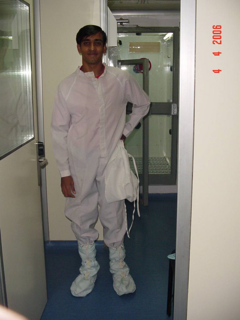
Fabrication of a chip is a very lengthy process and involves a series of sophisticated steps. These steps are performed by sophisticated equipment which is located in something called the clean room. Its called a clean room because it is totally dust free. To maintain the dust free atmosphere inside the room everyone who enters must wear an attire which covers him from head to toe. Also we need to pass through an Air cleaning chamber where air is sprayed on us so as to remove any dust particles that may be there.
Even a small amount of dust(which is nothing but impure silicon) can get transferred to the chip and spoil it. Hence care must be taken.
The device that we were going to fabricate was nothing compared to the ones being fabricated in the industry(where each chip has some million transistors-while our chip had just abt 100 capacitors at the end). But the very fact that we were doing something like that was enough to excite us.
So there we were..doing something abt which we had only read abt in the books or seen on TV..
(etching the wafer....growing oxide over silicon.... preparing mask using Photo resist...... metal deposition...... and then finally annealing the wafer).
Although these were not even half the steps needed for fabricating a full fledged transistor, but i guess this was enough for starters.
The following is a brief Description of the process(for those who are interested to know) :-
1 inch diameter silicon wafer is taken. This wafer is highly impure and consists of a lot of organic impurities and also some oxide layer due to natural oxidation. All these impurities are first removed by a process called etching where the chip(wafer) is placed in a concentrated solution of H2SO4(3 parts) and H2O2(1 part) and later in De-Ionised(DI) water.
After that the chip is ready for oxide growth. This is done by placing the wafer in a furnace maintained at a temperature of 1000 degC in an atmosphere consisting of dry O2. This is done for about 30 mins to obtain an oxide layer of 40nm thickness.
After that a mask is prepared and Aluminium deposition is done only at the places where we require the metal contacts(the upper plate of the capacitor)
After that the Chip is take to the other lab where Annealing is done in inert(Argon) atmosphere at 400 degC for abt 30 mins.
The whole process went on for some 5 hrs and we thoroughly enjoyed each and every moment of it. Today was one of those days when i really felt very very happy(and lucky) for coming to IISc. Really it was a moment to cherish. :-)
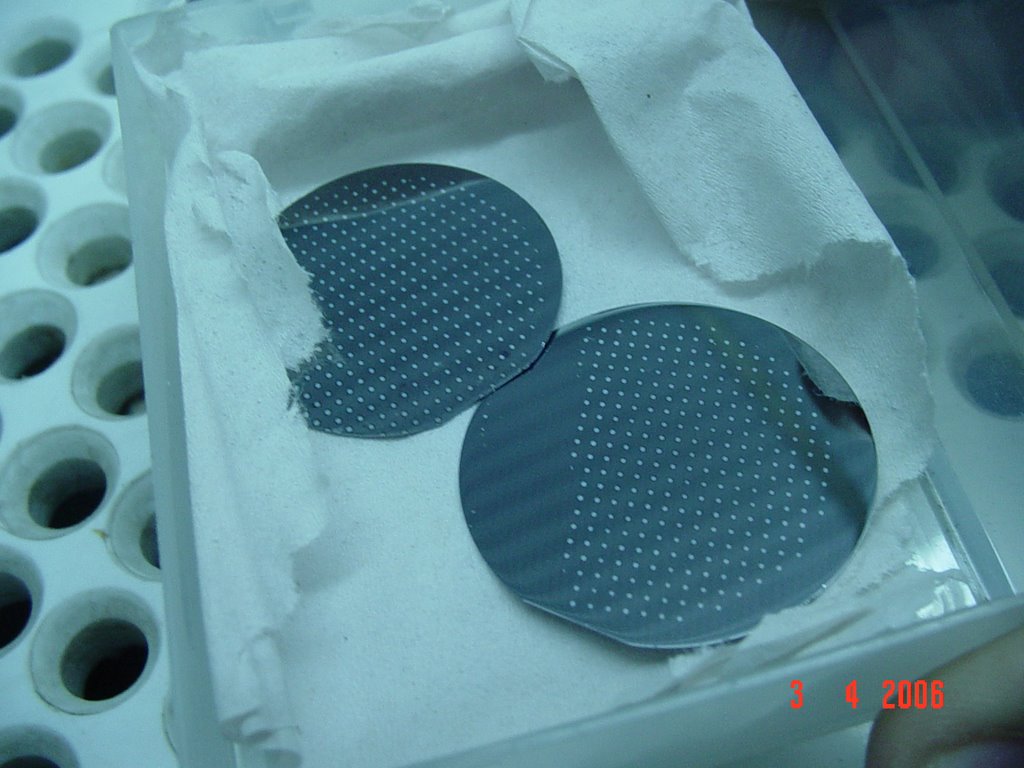
The following is an image of the chips at the end of the process.. the white dots that you see are the aluminium deposits. Each of them is a capacitor terminal(so abt 100 or more capacitors on one chip!!)... Now we need to do the characterization of some of them..that will be done in the coming week..so keep checking for the updates... :P
Hmmm ... will be awaiting for the zoom photos
ReplyDeletealya,
ReplyDeleteaatlu b adhu lakhvama time bagadyo ena karta vaanchvama thodu vadhare dhaayn aapu hot to 2 mark vadhare aavt ne.
Brilliant! i'll be undertaking a very similar project soon in iisc. this helped a lot. thanks!
ReplyDelete